Heterojunction is the "third generation mainstream technology" of photovoltaic cells, also known as the "ultimate platform-level technology" of photovoltaic cells. In terms of battery structure, heterojunction cells use N-type silicon wafers as substrates. There are huge differences between heterojunction cells and second-generation cells in terms of battery structure, process route and equipment, which makes them disruptive in technology.
Heterojunction + perovskite stacked cells are the "3.5 generation technology" of photovoltaic cells. Their battery structure is a combination of heterojunction cells and perovskite cells, which are connected in series through the TCO film layer; the upgrade of heterojunction cells to "heterojunction + perovskite" stacked cells can not only utilize the high efficiency characteristics of HJT, but also further improve the photoelectric conversion efficiency of the battery through the wide spectrum absorption characteristics of perovskite, and will not cause mutations in the process route and equipment of the heterojunction-related parts, thereby perfectly connecting the technological changes of photovoltaic cells.
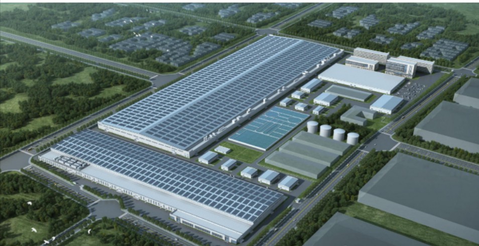
Recently, ASIACHEM learned that the 10GW heterojunction stacked high-efficiency battery production base project of Huainan Yiheng Photovoltaic Technology Co., Ltd. has started construction. The total investment of this project is about 6.6 billion yuan, and the total planned land area is about 538 acres. In the first phase, a 2.4GW heterojunction stacked high-efficiency battery production line and a 100MW perovskite stacked battery pilot line will be built.

According to the official microblog of "Yiheng Photovoltaic", Huainan Yiheng Photovoltaic Technology Co., Ltd. has introduced a first-line R&D and mass production technical team in the domestic photovoltaic industry, including 80 people with doctoral, master's and undergraduate degrees. The team has 11 years of R&D and mass production experience, with an average efficiency of more than 25.7% (ISFH standard) for mass-produced heterojunction cells, a module power of more than 745 watts, a mass-produced large-area perovskite cell efficiency of more than 22%, and a 166-size stacked cell efficiency of more than 27%. This project plans to use the future market-competitive G12 half-chip silicon wafer (210mm*105mm), pre-cut half-chip at the cutting end of the silicon wafer, and reduce the efficiency loss caused by the half-chip at the module end. The silicon wafers that have been tested and meet the requirements will be cleaned and textured to form a velvet surface, and then silicon film and TCO film will be deposited on the front and back of the silicon wafer after the texture, and electrodes will be formed through graphic processing, and finally heterojunction batteries will be produced.